SkyWatchMesh – UAP Intelligence Network

UAP Intelligence Network – Real-time monitoring of official UAP reports from government agencies and scientific institutions worldwide

Author:

  • Essential UAP Research Equipment: Building Your Sky Watching Setup

    🛸 Advanced UAP Detection: Research-Grade Equipment Guide

    Serious UAP research requires more than just looking up. After years of coordinating sky watching networks and analyzing anomalous phenomena, I’ve compiled the essential equipment list for credible UAP investigation and documentation.

    🔒 Secure Your Research

    Protect sensitive UAP data, witness testimonies, and research findings with military-grade encryption and secure hosting.

    **→ Secure Research Data with Surfshark VPN**

    FTC Disclosure: This post contains affiliate links. We may earn a commission if you purchase through these links at no additional cost to you. See our Affiliate Disclosure for details.

    📹 Video Documentation Systems

    **High-Resolution Cameras:** 4K capability minimum for detailed analysis. Sony A7S III or Canon R6 Mark II excel in low-light conditions crucial for night sky observation.

    **Telephoto Lenses:** 200-600mm zoom lenses capture distant objects. Image stabilization becomes critical at long focal lengths.

    **Infrared Cameras:** FLIR thermal imaging detects heat signatures invisible to conventional cameras. Essential for comprehensive spectrum analysis.

    🔭 Optical Observation Tools

    Professional-grade optics separate genuine anomalies from conventional aircraft, satellites, or atmospheric phenomena.

    **Telescopes:** Computerized mounts with GPS tracking maintain steady observation of moving objects. Celestron or Meade Schmidt-Cassegrain designs offer portability and power.

    🖥️ Research Infrastructure

    Reliable hosting and server infrastructure keeps your UAP research database accessible 24/7 for global collaboration.

    **→ Professional Hosting with Contabo**

    FTC Disclosure: This post contains affiliate links. We may earn a commission if you purchase through these links at no additional cost to you. See our Affiliate Disclosure for details.

    📡 Detection & Measurement Equipment

    **EMF Detectors:** Electromagnetic field meters detect anomalous energy signatures. Trifield TF2 or professional-grade gaussmeters provide quantifiable data.

    **Radiation Monitors:** Geiger counters identify radioactive anomalies sometimes associated with UAP encounters.

    **Weather Monitoring:** Comprehensive weather stations eliminate atmospheric explanations. Wind speed, humidity, and pressure readings contextualize observations.

    💻 Data Processing & Analysis

    Raw observations require sophisticated analysis to extract meaningful patterns and eliminate conventional explanations.

    **Image Analysis Software:** Specialized software identifies pixel patterns, motion vectors, and spectral analysis impossible with visual inspection alone.

    🧹 Research Environment

    Maintain clean, organized research spaces automatically so you can focus on the skies instead of housework.

    **→ Automated Cleaning with Ecovacs**

    FTC Disclosure: This post contains affiliate links. We may earn a commission if you purchase through these links at no additional cost to you. See our Affiliate Disclosure for details.

    🎯 Scientific Methodology

    Credible UAP research demands rigorous scientific protocols and peer review processes.

    **Documentation Standards:** Standardized observation forms ensure consistent data collection across different observers and locations.

    **Statistical Analysis:** Proper statistical methods identify significant patterns while avoiding false positive conclusions from random noise.

    Keep watching the skies – the truth is out there, but finding it requires dedication, proper equipment, and scientific methodology. 🌌

  • Arm joins Open Compute Project to build next-generation AI data center silicon

    Arm joins Open Compute Project to build next-generation AI data center silicon

    Chip designer Arm Holdings plc has announced it is joining the Open Compute Project to help address rising energy demands from

  • The business case for microsegmentation: Lower insurance costs, 33% faster ransomware response

    The business case for microsegmentation: Lower insurance costs, 33% faster ransomware response

    Network segmentation has been a security best practice for decades, yet for many reasons, not all network deployments have fully embraced the approach of microsegmentation. With ransomware attacks becoming increasingly sophisticated and cyber insurance underwriters paying closer attention to network architecture, microsegmentation is transitioning from nice to have to business imperative.

    New research from Akamai examines how organizations are approaching microsegmentation adoption, implementation challenges, and the tangible benefits they’re seeing. The data reveals a significant gap between awareness and execution, but it also shows clear financial and operational incentives for network teams willing to make the transition. Key findings from Akamai’s Segmentation Impact Study, which surveyed 1,200 security and technology leaders worldwide, include:

    • Only 35% of organizations have implemented microsegmentation across their network environment despite 90% having adopted some form of segmentation.
    • Organizations with more than $1 billion in revenue saw ransomware containment time reduced by 33% after implementing microsegmentation.
    • 60% of surveyed organizations received lower insurance premiums tied to segmentation maturity.
    • 75% of insurers now assess segmentation posture during underwriting.
    • Network complexity (44%), visibility gaps (39%) and operational resistance (32%) remain the primary barriers to adoption.
    • Half of non-adopters plan to implement microsegmentation within two years, while 68% of current users expect to increase investment.

    “I believe the biggest surprise in the data was the effectiveness of microsegmentation when used as a tool for containing breaches,” Garrett Weber, field CTO for enterprise security at Akamai, told Network World. “We often think of segmentation as a set-it-and-forget-it solution, but with microsegmentation bringing the control points to the workloads themselves, it offers organizations the ability to quickly contain breaches.”

    Why traditional segmentation falls short

    Microsegmentation applies security policies at the individual workload or application level rather than at the network perimeter or between large network zones.

    Weber challenged network admins who feel their current north-south segmentation is adequate. “I would challenge them to really try and assess and understand the attacker’s ability to move laterally within the segments they’ve created,” he said. “Without question they will find a path from a vulnerable web server, IoT device or endpoint that can allow an attacker to move laterally and access sensitive information within the environment.”

    The data supports this assessment. Organizations implementing microsegmentation reported multiple benefits beyond ransomware containment. These include protecting critical assets (74%), responding faster to incidents (56%) and safeguarding against internal threats (57%).

    Myths and misconceptions about microsegmentation

    The report detailed a number of reasons why organizations have not properly deployed microsegmentation. Network complexity topped the list of implementation barriers at 44%, but Weber questioned the legitimacy of that barrier.

    “Many organizations believe their network is too complex for microsegmentation, but once we dive into their infrastructure and how applications are developed and deployed, we typically see that microsegmentation solutions are a better fit for complex networks than traditional segmentation approaches,” Weber said. “There is usually a misconception that microsegmentation solutions are reliant on a virtualization platform or cannot support a variety of cloud or kubernetes deployments, but modern microsegmentation solutions are built for simplifying network segmentation within complex environments.”

    Another common misconception is that implementing microsegmentation solutions will impact performance of applications and potentially create outages from poor policy creation. “Modern microsegmentation solutions are designed to minimize performance impacts and provide the proper workflows and user experiences to safely implement security policies at scale,” Weber said.

    Insurance benefits create business case

    Cyber insurance has emerged as an unexpected driver for microsegmentation adoption. The report states that 85% of organizations using microsegmentation find audit reporting easier. Of those, 33% reported reduced costs associated with attestation and assurance. More significantly, 74% believe stronger segmentation increases the likelihood of insurance claim approval.

    For network teams struggling to justify the investment to leadership, the insurance angle can provide concrete financial benefits: 60% of surveyed organizations said they received premium reductions as a result of improved segmentation posture.

    Beyond insurance savings and faster ransomware response, Weber recommends network admins track several operational performance indicators to demonstrate ongoing value.

    Attack surface reduction of critical applications or environments can provide a clear security posture metric. Teams should also monitor commonly abused ports and services like SSH and Remote Desktop. The goal is tracking how much of that traffic is being analyzed and controlled by policy.

    For organizations integrating microsegmentation into SOC playbooks, time to breach identification and containment can offer a direct measure of incident response improvement.

    AI can help ease adoption

    Since it’s 2025, no conversation about any technology can be complete without mention of AI. For its part, Akamai is investing in AI to help improve the user experience with microsegmentation. 

    Weber outlined three specific areas where AI is improving the microsegmentation experience. First, AI can automatically identify and tag workloads. It does this by analyzing traffic patterns, running processes and other data points. This eliminates manual classification work.

    Second, AI assists in recommending security policies faster and with more granularity than most network admins and application owners can achieve manually. This capability is helping organizations implement policies at scale.

    Third, natural language processing through AI assistants helps users mine and understand the significant amount of data microsegmentation solutions collect. This works regardless of their experience level with the platform.

    Implementation guidance

    According to the survey, 50% of non-adopters plan to implement microsegmentation within the next 24 months. For those looking to implement microsegmentation effectively, the report outlines four key steps :

    • Achieve deep, continuous visibility: Map workloads, applications and traffic patterns in real time to surface dependencies and risks before designing policies
    • Design policies at the workload level: Apply fine-grained controls that limit lateral movement and enforce zero-trust principles across hybrid and cloud environments
    • Simplify deployment with scalable architecture: Adopt solutions that embed segmentation into existing infrastructure without requiring a full network redesign
    • Strengthen governance and automation: Align segmentation with security operations and compliance goals, using automation to sustain enforcement and accelerate maturity

    🛸 Recommended Intelligence Resource

    As UAP researchers and tech enthusiasts, we’re always seeking tools and resources to enhance our investigations and stay ahead of emerging technologies. Check out this resource that fellow researchers have found valuable.

    → EHarmony

    FTC Disclosure: This post contains affiliate links. We may earn a commission if you purchase through these links at no additional cost to you. See our Affiliate Disclosure for details.

  • Electrifying Everything Will Require Multiphysics Modeling

    Electrifying Everything Will Require Multiphysics Modeling

    A prototyping problem is emerging in today’s efforts to electrify everything. What works as a lab-bench mockup breaks in reality. Harnessing and safely storing energy at grid scale and in cars, trucks, and planes is a very hard problem that simplified models sometimes can’t touch.

    “In electrification, at its core, you have this combination of electromagnetic effects, heat transfer, and structural mechanics in a complicated interplay,” says Bjorn Sjodin, senior vice president of product management at the Stockholm-based software company COMSOL.

    COMSOL is an engineering R&D software company that seeks to simulate not just a single phenomenon—for instance, the electromagnetic behavior of a circuit—but rather all the pertinent physics that needs to be simulated for developing new technologies in real-world operating conditions.

    Engineers and developers gathered in Burlington, Mass. on 8-10 Oct. for COMSOL’s annual Boston conference, where they discussed engineering simulations via multiple simultaneous physics packages. And multiphysics modeling, as the emerging field is called, has emerged as a component of electrification R&D that is becoming more than just nice-to-have.

    “Sometimes, I think some people still see simulation as a fancy R&D thing,” says Niloofar Kamyab, a chemical engineer and applications manager at COMSOL. “Because they see it as a replacement for experiments. But no, experiments still need to be done, though experiments can be done in a more optimized and effective way.”

    Can Multiphysics Scale Electrification?

    Multiphysics, Kamyab says, can sometimes be only half the game.

    “I think when it comes to batteries, there is another attraction when it comes to simulation,” she says. “It’s multi-scale—how batteries can be studied across different scales. You can get in-depth analysis that, if not very hard, I would say is impossible to do experimentally.”

    In part, this is because batteries reveal complicated behaviors (and runaway reactions) at the cell level but also in unpredictable new ways at the battery-pack level as well.

    “Most of the people who do simulations of battery packs, thermal management is one of their primary concerns,” Kamyab says. “You do this simulation so you know how to avoid it. You recreate a cell that is malfunctioning.” She adds that multiphysics simulation of thermal runaway enables battery engineers to safely test how each design behaves in even the most extreme conditions—in order to stop any battery problems or fires before they could happen.

    Wireless charging systems are another area of electrification, with their own thermal challenges. “At higher power levels, localized heating of the coil changes its conductivity,” says Nirmal Paudel, a lead engineer at Veryst Engineering, an engineering consulting firm based in Needham, Mass. And that, he notes, in turn can change the entire circuit as well as the design and performance of all the elements that surround it.

    Electric motors and power converters require similar simulation savvy. According to electrical engineer and COMSOL senior application engineer Vignesh Gurusamy, older ways of developing these age-old electrical workhorse technologies are proving less useful today. “The recent surge in electrification across diverse applications demands a more holistic approach as it enables the development of new optimal designs,” Gurusamy says.

    And freight transportation: “For trucks, people are investigating, Should we use batteries? Should we use fuel cells?” Sjodin says. “Fuel cells are very multiphysics friendly—fluid flow, heat transfer, chemical reactions, and electrochemical reactions.”

    Lastly, there’s the electric grid itself. “The grid is designed for a continuous supply of power,” Sjodin says. “So when you have power sources [like wind and solar] shutting off and on all the time, you have completely new problems.”

    Multiphysics in Battery and Electric Motor Design

    Taking such an all-in approach to engineering simulations can yield unanticipated upsides as well, says Kamyab. Berlin-based automotive engineering company IAV, for example, is developing powertrain systems that integrate multiple battery formats and chemistries in a single pack. “Sodium ion cannot give you the energy that lithium ion can give,” Kamyab says. “So they came up with a blend of chemistries, to get the benefits of each, and then designed a thermal management that matches all the chemistries.”

    Jakob Hilgert, who works as a technical consultant at IAV, recently contributed to a COMSOL industry case study. In it, Hilgert described the design of a dual-chemistry battery pack that combines sodium-ion cells with a more costly lithium solid-state battery.

    Hilgert says that using multiphysics simulation enabled the IAV team to play the two chemistries’ different properties off of each other. “If we have some cells that can operate at high temperatures and some cells that can operate at low temperatures, it is beneficial to take the exhaust heat of the higher-running cells to heat up the lower-running cells, and vice versa,” Hilgert said. “That’s why we came up with a cooling system that shifts the energy from cells that want to be in a cooler state to cells that want to be in a hotter state.”

    According to Sjodin, IAV is part of a larger trend in a range of industries that are impacted by the electrification of everything. “Algorithmic improvements and hardware improvements multiply together,” he says. “That’s the future of multiphysics simulation. It will allow you to simulate larger and larger, more realistic systems.”

    According to Gurusamy, GPU accelerators and surrogate models allow for bigger jumps in electric motor capabilities and efficiencies. Even seemingly simple components like the windings of copper wire in a motor core (called stators) provide parameters that multiphysics can optimize.

    “A primary frontier in electric motor development is pushing power density and efficiency to new heights, with thermal management emerging as a key challenge,” Gurusamy says. “Multiphysics models that couple electromagnetic and thermal simulations incorporate temperature-dependent behavior in stator windings and magnetic materials.”

    Simulation is also changing the wireless charging world, Paudel says. “Traditional design cycles tweak coil geometry,” he says. “Today, integrated multiphysics platforms enable exploration of new charging architectures,” including flexible charging textiles and smart surfaces that adapt in real-time.

    And batteries, according to Kamyab, are continuing a push toward higher power densities and lower price points. Which is changing not just the industries where batteries are already used, like consumer electronics and EVs. Higher-capacity batteries are also driving new industries like electric vertical take-off and landing aircraft (eVTOLs).

    “The reason that many ideas that we had 30 years ago are becoming a reality is now we have the batteries to power them,” Kamyab says. “That was the bottleneck for many years. … And as we continue to push battery technology forward, who knows what new technologies and applications we’re making possible next.”

    🛸 Recommended Intelligence Resource

    As UAP researchers and tech enthusiasts, we’re always seeking tools and resources to enhance our investigations and stay ahead of emerging technologies. Check out this resource that fellow researchers have found valuable.

    → Ecovacs

  • You Can Cool Chips With Lasers?!?!

    Modern high-performance chips are marvels of engineering, containing tens of billions of transistors. The problem is, you can’t use them all at once. If you did, you would create hot spots—high temperatures concentrated in tiny areas—with power densities nearing those found at the surface of the sun. This has led to a frustrating paradox known as dark silicon, a term coined by computer architects to describe the growing portion of a chip that must be kept powered down. Up to 80 percent of the transistors on a modern chip must remain “dark” at any given moment to keep the chip from sizzling. We are building supercomputers on a sliver of silicon but only using a fraction of their potential. It’s like building a skyscraper and being able to use only the first 10 floors.

    For years, the industry has battled this thermal limit with bigger fans and more complex liquid cooling systems. But these are fundamentally Band-Aid solutions. Whether using air or liquid, they rely on pulling heat away from the chip’s surface. The heat must first conduct through the silicon to the cooling plate, creating a thermal bottleneck that simply cannot be overcome at the power densities of future chips. Hot spots on today’s chips produce tens of watts per square millimeter, and they pop up in various places on the chip at different times during computations. Air and liquid cooling struggle to focus their efforts at just the hot spots, when and where they appear—they can only try to cool the whole thing en masse.

    We at St. Paul, Minn.–based startup Maxwell Labs are proposing a radical new approach: What if, instead of just moving heat, you could make it disappear? The technology, which we call photonic cooling, is capable of converting heat directly into light—cooling the chip from the inside out. The energy can then be recovered and recycled back into useful electric power. With this approach, instead of cooling the whole chip uniformly, we can target hot spots as they form, with laser precision. Fundamentally, this technique could cool hot spots of thousands of watts per square millimeter, orders of magnitude better than today’s chips are cooled.

    The Physics of Cooling With Light

    Lasers are usually thought of as sources of heat, and for good reason—they are most commonly used for cutting materials or transferring data. But under the right circumstances, laser light can induce cooling. The secret lies in a luminescent process known as fluorescence.

    Fluorescence is the phenomenon behind the familiar glow of highlighter markers, coral reefs, and white clothes under black-light illumination. These materials absorb high-energy light—usually in the ultraviolet—and reemit lower energy light, often in the visible spectrum. Because they absorb higher energy than they emit, the difference often results in heating up the material. However, under certain, very niche conditions, the opposite can happen: A material can absorb low-energy photons and emit higher-energy light, cooling down in the process.

    To cool computer chips with lasers, the team at Maxwell Labs plans to place a grid of photonic cold plates on top of the chip substrate. In their demo setup, a thermal camera detects hot spots coming from the chip. A laser then shines onto the photonic cold plate next to the hot spot, stimulating the photonic process that results in cooling. The photonic cold plate [inset] consists of a coupler that guides light in and out of the plate, the extractor where anti-Stokes fluorescence occurs, the back reflector that prevents light from entering the computer chip, and a sensor that is designed to detect hot spots.GygInfographics.com

    The reemission is higher energy because it combines the energy from the incoming photons with phonons, vibrations in the crystal lattice of a material. This phenomenon is called anti-Stokes cooling, and it was first demonstrated in a solid back in 1995 when a team of scientists cooled an ytterbium-doped fluoride glass sample with laser light.

    The choice of ytterbium as a dopant was not random: Anti-Stokes cooling works only under carefully engineered conditions. The absorbing material must be structured so that for nearly every absorbed photon a higher-energy photon will be emitted. Otherwise, other mechanisms will kick in, heating rather than cooling the sample. Ions of ytterbium and other such lanthanides have the right structure of electron orbitals to facilitate this process. For a narrow range of laser wavelengths shining on the material, the ions can effectively absorb the incident light and use phonons to trigger emission of higher-energy light. This reemitted, extracted thermal light needs to escape the material quickly enough to not be absorbed again, which would otherwise cause heating.

    To date, lab-based approaches have achieved up to 90 watts of cooling power in ytterbium-doped silica glass. As impressive as that is, to achieve the transformative effects on high-performance chips that we anticipate, we need to boost the cooling capacity by many orders of magnitude. Achieving this requires integration of the photonic cooling mechanism onto a thin-film, chip-scale photonic cold plate. Miniaturization not only enables more precise spatial targeting of hot spots due to the tightly focused beam, but is a crucial element for pushing the physics of laser cooling toward high-power and high-efficiency regimes. The thinner layer also makes it less likely that the light will get reabsorbed before escaping the film, avoiding heating. And, by engineering the materials at the scale of the wavelength of light, it allows for increased absorption of the incoming laser beam.

    Photonic Cold-Plate Technology

    In our lab, we are developing a way to harness photonic cooling to tackle the heat from today’s and future CPUs and GPUs. Our photonic cold plate is designed to sense areas of increasing power density (emerging hot spots) and then couple light efficiently into a nearby region that cools the hot spots down to a target temperature.

    The photonic cold plate has several components: first the coupler, which couples the incoming laser light into the other components; then, the microrefrigeration region, where the cooling actually happens; next, the back reflector, which prevents light from hitting the CPU or GPU directly; and last a sensor, which detects the hot spots as they form.

    The laser shines onto the targeted area from above through the coupler: a kind of lens that focuses the incoming laser light onto a microrefrigeration region. The coupler simultaneously channels the inbound heat-carrying fluorescent light out of the chip. The microrefrigeration region, which we call the extractor, is where the real magic happens: The specially doped thin film undergoes anti-Stokes fluorescence.

    To prevent the incoming laser light and fluorescent light from entering the actual chip and heating the electronics, the photonic cold plate incorporates a back reflector.

    Crucially, cooling occurs only when, and where, the laser is shining onto the cold plate. By choosing where to shine the laser, we can target hot spots as they appear on the chip. The cold plate includes a thermal sensor that detects hot spots, allowing us to steer the laser toward them.

    Designing this whole stack is a complex, interconnected problem with many adjustable parameters, including the exact shape of the coupler, the material and doping level of the extraction region, and the thickness and number of layers in the back reflector. To optimize the cold plate, we are deploying a multiphysics simulation model combined with inverse design tools that let us search the vast set of possible parameters. We are leveraging these tools in the hope of improving cooling power densities by two orders of magnitude, and we are planning larger simulations to achieve bigger improvements still.

    Collaborating with our partners at the University of New Mexico in Albuquerque, the University of St. Thomas in St. Paul, Minn., and Sandia National Laboratories in Albuquerque, we are building a demonstration version of photonic cooling at our lab in St. Paul. We are assembling an array of small photonic cold plates, each a square millimeter in size, tiled atop various CPUs. For demonstration purposes, we use an external thermal camera to sense the hot spots coming from the chips. When a hot spot begins to appear, a laser is directed onto the photonic cold plate tile directly atop it, extracting its heat. Our first iteration of the cold plate used ytterbium ion doping, but we are now experimenting with a variety of other dopants that we believe will achieve much higher performance.

    In an upcoming integrated implementation of this demo, the photonic cold plates will consist of finer tiles—about 100 by 100 micrometers. Instead of a free-space laser, light from a fiber will be routed to these tiles by an on-chip photonic network. Which tiles are activated by the laser light will depend on where and when hot spots form, as measured by the sensor.

    Eventually, we hope to collaborate with CPU and GPU manufacturers to integrate the photonic cold plates within the same package as the chip itself, allowing us to get the crucial extractor layer closer to the hot spots and increase the cooling capacity of the device.

    The Laser-Cooled Chip and the Data Center

    To understand the impact of our photonic cooling technology on current and future data centers, we have performed an analysis of the thermodynamics of laser cooling combined with and compared to air and liquid cooling approaches. Preliminary results show that even a first-generation laser-cooling setup can dissipate twice the power of purely air and liquid cooling systems. This drastic improvement in cooling capability would allow for several key changes to chip and target=”_self”>expected only to get worse. The ability to overcome this bottleneck would allow for higher clocking frequencies on the same chips. This opens up the possibility of improving chip performance without directly increasing transistor densities, giving much needed headroom for Moore’s Law to continue to progress.

    The demo setup at Maxwell Labs demonstrates how current computer chips can be cooled with lasers. A photonic cold plate is placed on top of the chip. A thermal camera images the hot spots coming from the chip, and a laser is directed at the photonic cold plate directly above the hot spot.Maxwell Labs

    Third, this technology makes 3D integration thermally manageable. Because laser-assisted cooling pinpoints the hot spots, it can more readily remove heat from a 3D stack in a way that today’s cooling tech can’t. Adding a photonic cold plate to each layer in a 3D integrated stack would take care of cooling the whole stack, making 3D chip design much more straightforward.

    Fourth, laser cooling is more efficient than air cooling systems. An even more tantalizing result of the removal of heat from hot spots is the ability to keep the chip at a uniform temperature and greatly reduce the overall power consumption of convective cooling systems. Our calculations show that, when combined with air cooling, reductions in overall energy consumption of more than 50 percent for current generation chips are possible, and significantly larger savings would be achieved for future chips.

    What’s more, laser cooling allows for recovering a much higher fraction of waste energy than is possible with air or liquid cooling. Recirculating hot liquid or air to heat nearby houses or other facilities is possible in certain locations and climates, but the recycling efficiency of these approaches is limited. With photonic cooling, the light emitted via anti-Stokes fluorescence can be recovered by re-collecting the light into fiber-optic cables and then converting it to electricity through thermophotovoltaics, leading to upwards of 60 percent energy recovery.

    With this fundamentally new approach to cooling, we can rewrite the rules by which chips and data centers are designed. We believe this could be what enables the continuation of Moore’s Law, as well as the power savings at the data-center level that could greenlight the intelligence explosion we’re starting to see today.

    The Path to Photonic Cooling

    While our results are highly promising, several challenges remain before this technology can become a commercial reality. The materials we are currently using for our photonic cold plates meet basic requirements, but continued development of higher efficiency laser-cooling materials will improve system performance and make this an increasingly economically attractive proposition. To date, only a handful of materials have been studied and made pure enough to allow laser cooling. We believe that miniaturization of the photonic cold plate, aided by progress in optical engineering and thin-film materials processing, will have similarly transformative effects on this technology as it has for the transistor, solar cells, and lasers.

    We’re going to need to codesign the processors, packages, and cooling systems to maximize benefits. This will require close collaboration across the traditionally siloed semiconductor ecosystem. We are working with industry partners to try to facilitate this codesign process.

    Transitioning from a lab-based setup to high-volume commercial manufacturing will require us to develop efficient processes and specialized equipment. Industry-wide adoption necessitates new standards for optical interfaces, safety protocols, and performance metrics.

    Although there is much to be done, we do not see any fundamental obstacles now to the large-scale adoption of photonic cooling technology. In our current vision, we anticipate the early adoption of the technology in high-performance computing and AI training clusters before 2027, showing an order-of-magnitude improvement in performance per watt of cooling. Then, between 2028 and 2030, we hope to see mainstream data-center deployment, with an accompanied reduction in IT energy consumption of 40 percent while doubling compute capacity. Finally, after 2030 we foresee that ubiquitous deployment, from hyperscale to edge, will enable new computing paradigms limited only by algorithmic efficiency rather than thermal constraints.

    For over two decades, the semiconductor industry has grappled with the looming threat of dark silicon. Photonic cooling offers not merely a solution to that challenge but a fundamental reimagining of the relationship between performance, computation, and energy. By converting waste heat directly into useful photons and ultimately back into electricity, this technology transforms thermal management from a necessary evil into a valuable resource.

    The future of computing is photonic, efficient, and brilliantly cool.

    🛸 Recommended Intelligence Resource

    As UAP researchers and tech enthusiasts, we’re always seeking tools and resources to enhance our investigations and stay ahead of emerging technologies. Check out this resource that fellow researchers have found valuable.

    → contabo

  • Oct. 16, 1975: The first GOES satellite launches

    A joint project of NASA and the National Oceanic and Atmospheric Administration (NOAA), the Geostationary Operational Environmental Satellites (GOES) program provides continuous monitoring of weather both on Earth and in space. The GOES satellites map lightning activity, measure and image atmospheric conditions, and track solar activity and space weather. This constant flow of data isContinue reading “Oct. 16, 1975: The first GOES satellite launches”

    The post Oct. 16, 1975: The first GOES satellite launches appeared first on Astronomy Magazine.

    🛸 Recommended Intelligence Resource

    As UAP researchers and tech enthusiasts, we’re always seeking tools and resources to enhance our investigations and stay ahead of emerging technologies. Check out this resource that fellow researchers have found valuable.

    → contabo

  • Scalar Physics, Alien Messages, and Bottomless Holes: Bizarre but Thought-Provoking Conspiracies!

    Scalar Physics, Alien Messages, and Bottomless Holes: Bizarre but Thought-Provoking Conspiracies!

    The conspiracy world is a strange place to step into. It is often a strange and potentially dangerous mix of obscured partial truths, bizarre claims that border on the preposterous, and muddied and distorted facts, statistics, and statements. Perhaps because of this, it is also a world where individuals or groups can hijack or even outright invent conspiracies for their own ends, a situation that potentially affects us all.

    🛸 Recommended Intelligence Resource

    As UAP researchers and tech enthusiasts, we’re always seeking tools and resources to enhance our investigations and stay ahead of emerging technologies. Check out this resource that fellow researchers have found valuable.

    → Ecovacs

  • Oracle’s big bet for AI: Zettascale10

    Oracle’s big bet for AI: Zettascale10

    Oracle Cloud Infrastructure (OCI) is not just going all-in on AI, but on AI at incredible scale.

    This week, the company announced what it calls the largest AI supercomputer in the cloud, OCI Zettascale10. The multi-gigawatt architecture links hundreds of thousands of Nvidia GPUs to deliver what OCI calls “unprecedented” performance.

    The supercomputer will serve as the backbone for the ambitious, yet somewhat embattled, $500 billion Stargate project.

    “The platform offers benefits such as accelerated performance, enterprise scalability, and operational efficiency attuned towards the needs of industry-specific AI applications,” Yaz Palanichamy, senior advisory analyst at Info-Tech Research Group, told Network World.

    How Oracle’s new supercomputer works

    Oracle’s new supercomputer stitches together hundreds of thousands of Nvidia GPUs across multiple data centers, essentially forming multi-gigawatt clusters. This allows the architecture to deliver up to 10X more zettaFLOPS of peak performance: An “unprecedented” 16 zettaFLOPS, the company claims.

    To put that in perspective, a zettaFLOP (a 1 followed by 21 zeroes) can perform one sextillion FLOPS (floating point operations per second), allowing systems to perform intensely complex computations, like those calculated by the most advanced AI and machine learning (ML) systems. That compares to computers working at gigaflop (1 followed by 9 zeroes) or exaFLOP (1 followed by 18 zeroes) speeds.

    “OCI Zettascale10 was designed with the goal of integrating large-scale generative AI use cases, including training and running large language models,” said Info-Tech’s Palanichamy.

    Oracle also introduced new capabilities in Oracle Acceleron, its OCI networking stack, that it said helps customers run workloads more quickly and cost-effectively. They include dedicated network fabrics, converged NICs, and host-level zero-trust packet routing that Oracle says can double network and storage throughput while cutting latency and cost.

    Oracle’s zettascale supercomputer is built on the Acceleron RoCE (RDMA over Converged Ethernet) architecture and Nvidia AI infrastructure. This allows it to deliver what Oracle calls “breakthrough” scale, “extremely low” GPU-to-GPU latency, and improved price/performance, cluster use, and overall reliability.

    The new architecture has a “wide, shallow, resilient” fabric, according to Oracle, and takes advantage of switching capabilities built into modern GPU network interface cards (NICs). This means it can connect to multiple switches at the same time, but each switch stays on its own isolated network plane.

    Customers can thus deploy larger clusters, faster, while running into fewer stalls and checkpoint restarts, because traffic can be shifted to different network planes and re-routed when the system encounters unstable or contested paths.

    The architecture also features power-efficient optics and is “hyper-optimized” for density, as its clusters are located in large data center campuses within a two-kilometer radius, Oracle said.

    “The highly-scalable custom design maximizes fabric-wide performance at gigawatt scale while keeping most of the power focused on compute,” said Peter Hoeschele, VP for infrastructure and industrial compute at OpenAI.

    OCI is now taking orders for OCI Zettascale10, which will be available in the second half of 2026. The company plans to offer multi-gigawatt deployments, initially targeting those with up to 800,000 Nvidia GPUs.

    But is it really necessary?

    While this seems like an astronomical amount of compute, “there are customers for it,” particularly envelope-pushing companies like OpenAI, said Alvin Nguyen, a senior analyst at Forrester.

    He pointed out that most AI models have been trained on text, essentially at this point comprising “all of human-written history.” Now, though, systems are ingesting large and compute-heavy files including images, audio, and video. “Inferencing is expected to grow even bigger than the training steps,” he said.

    And, ultimately, it does take a while for new AI factories/systems like OCI Zettascale10 to be produced at volume, he noted, which could lead to potential issues. “There is a concern in terms of what it means if [enterprises] don’t have enough supply,” said Nguyen. However, “a lot of it is unpredictable.”

    Info-Tech’s Palanichamy agreed that fears are ever-present around large-scale GPU procurement, but pointed to the Oracle-AMD partnership announced this week, aimed at achieving next-gen AI scalability.

    “It is a promising next step for safeguarding and balancing extreme scale in GPU demand, alongside enabling energy efficiency for large-scale AI training and inference,” he said.

    Advice to enterprises who can’t afford AI factories: ‘Get creative’

    Nguyen pointed out that, while OpenAI is a big Oracle partner, the bulk of the cloud giant’s customers aren’t research labs, they’re everyday enterprises that don’t necessarily need the latest and greatest.

    Their more modest requirements offer those customers an opportunity to identify other ways to improve performance and speed, such as by simply updating software stacks. It’s also a good time for them to analyze their supply chain and supply chain management capabilities.

    “They should be making sure they’re very aware of their supply chain, vendors, partners, making sure they can get access to as much as they can,” Nguyen advised.

    Not many companies can afford their own AI mega-factories, he pointed out, but they can take advantage of mega-factories owned and run by others. Look to partners, pursue other cloud options, and get creative, he said.

    There is no doubt that, as with the digital divide, there is a growing “AI divide,” said Nguyen. “Not everyone is going to be Number One, but you don’t have to be. It’s being able to execute when that opportunity arises.”

    More Oracle news

    🛸 Recommended Intelligence Resource

    As UAP researchers and tech enthusiasts, we’re always seeking tools and resources to enhance our investigations and stay ahead of emerging technologies. Check out this resource that fellow researchers have found valuable.

    → hotel-deals

    FTC Disclosure: This post contains affiliate links. We may earn a commission if you purchase through these links at no additional cost to you. See our Affiliate Disclosure for details.

  • Oracle’s big bet for AI: Zettascale10

    Oracle’s big bet for AI: Zettascale10

    Oracle Cloud Infrastructure (OCI) is not just going all-in on AI, but on AI at incredible scale.

    This week, the company announced what it calls the largest AI supercomputer in the cloud, OCI Zettascale10. The multi-gigawatt architecture links hundreds of thousands of Nvidia GPUs to deliver what OCI calls “unprecedented” performance.

    The supercomputer will serve as the backbone for the ambitious, yet somewhat embattled, $500 billion Stargate project.

    “The platform offers benefits such as accelerated performance, enterprise scalability, and operational efficiency attuned towards the needs of industry-specific AI applications,” Yaz Palanichamy, senior advisory analyst at Info-Tech Research Group, told Network World.

    How Oracle’s new supercomputer works

    Oracle’s new supercomputer stitches together hundreds of thousands of Nvidia GPUs across multiple data centers, essentially forming multi-gigawatt clusters. This allows the architecture to deliver up to 10X more zettaFLOPS of peak performance: An “unprecedented” 16 zettaFLOPS, the company claims.

    To put that in perspective, a zettaFLOP (a 1 followed by 21 zeroes) can perform one sextillion FLOPS (floating point operations per second), allowing systems to perform intensely complex computations, like those calculated by the most advanced AI and machine learning (ML) systems. That compares to computers working at gigaflop (1 followed by 9 zeroes) or exaFLOP (1 followed by 18 zeroes) speeds.

    “OCI Zettascale10 was designed with the goal of integrating large-scale generative AI use cases, including training and running large language models,” said Info-Tech’s Palanichamy.

    Oracle also introduced new capabilities in Oracle Acceleron, its OCI networking stack, that it said helps customers run workloads more quickly and cost-effectively. They include dedicated network fabrics, converged NICs, and host-level zero-trust packet routing that Oracle says can double network and storage throughput while cutting latency and cost.

    Oracle’s zettascale supercomputer is built on the Acceleron RoCE (RDMA over Converged Ethernet) architecture and Nvidia AI infrastructure. This allows it to deliver what Oracle calls “breakthrough” scale, “extremely low” GPU-to-GPU latency, and improved price/performance, cluster use, and overall reliability.

    The new architecture has a “wide, shallow, resilient” fabric, according to Oracle, and takes advantage of switching capabilities built into modern GPU network interface cards (NICs). This means it can connect to multiple switches at the same time, but each switch stays on its own isolated network plane.

    Customers can thus deploy larger clusters, faster, while running into fewer stalls and checkpoint restarts, because traffic can be shifted to different network planes and re-routed when the system encounters unstable or contested paths.

    The architecture also features power-efficient optics and is “hyper-optimized” for density, as its clusters are located in large data center campuses within a two-kilometer radius, Oracle said.

    “The highly-scalable custom design maximizes fabric-wide performance at gigawatt scale while keeping most of the power focused on compute,” said Peter Hoeschele, VP for infrastructure and industrial compute at OpenAI.

    OCI is now taking orders for OCI Zettascale10, which will be available in the second half of 2026. The company plans to offer multi-gigawatt deployments, initially targeting those with up to 800,000 Nvidia GPUs.

    But is it really necessary?

    While this seems like an astronomical amount of compute, “there are customers for it,” particularly envelope-pushing companies like OpenAI, said Alvin Nguyen, a senior analyst at Forrester.

    He pointed out that most AI models have been trained on text, essentially at this point comprising “all of human-written history.” Now, though, systems are ingesting large and compute-heavy files including images, audio, and video. “Inferencing is expected to grow even bigger than the training steps,” he said.

    And, ultimately, it does take a while for new AI factories/systems like OCI Zettascale10 to be produced at volume, he noted, which could lead to potential issues. “There is a concern in terms of what it means if [enterprises] don’t have enough supply,” said Nguyen. However, “a lot of it is unpredictable.”

    Info-Tech’s Palanichamy agreed that fears are ever-present around large-scale GPU procurement, but pointed to the Oracle-AMD partnership announced this week, aimed at achieving next-gen AI scalability.

    “It is a promising next step for safeguarding and balancing extreme scale in GPU demand, alongside enabling energy efficiency for large-scale AI training and inference,” he said.

    Advice to enterprises who can’t afford AI factories: ‘Get creative’

    Nguyen pointed out that, while OpenAI is a big Oracle partner, the bulk of the cloud giant’s customers aren’t research labs, they’re everyday enterprises that don’t necessarily need the latest and greatest.

    Their more modest requirements offer those customers an opportunity to identify other ways to improve performance and speed, such as by simply updating software stacks. It’s also a good time for them to analyze their supply chain and supply chain management capabilities.

    “They should be making sure they’re very aware of their supply chain, vendors, partners, making sure they can get access to as much as they can,” Nguyen advised.

    Not many companies can afford their own AI mega-factories, he pointed out, but they can take advantage of mega-factories owned and run by others. Look to partners, pursue other cloud options, and get creative, he said.

    There is no doubt that, as with the digital divide, there is a growing “AI divide,” said Nguyen. “Not everyone is going to be Number One, but you don’t have to be. It’s being able to execute when that opportunity arises.”

    🛸 Recommended Intelligence Resource

    As UAP researchers and tech enthusiasts, we’re always seeking tools and resources to enhance our investigations and stay ahead of emerging technologies. Check out this resource that fellow researchers have found valuable.

    → Ecovacs

  • Three options for wireless power in the enterprise

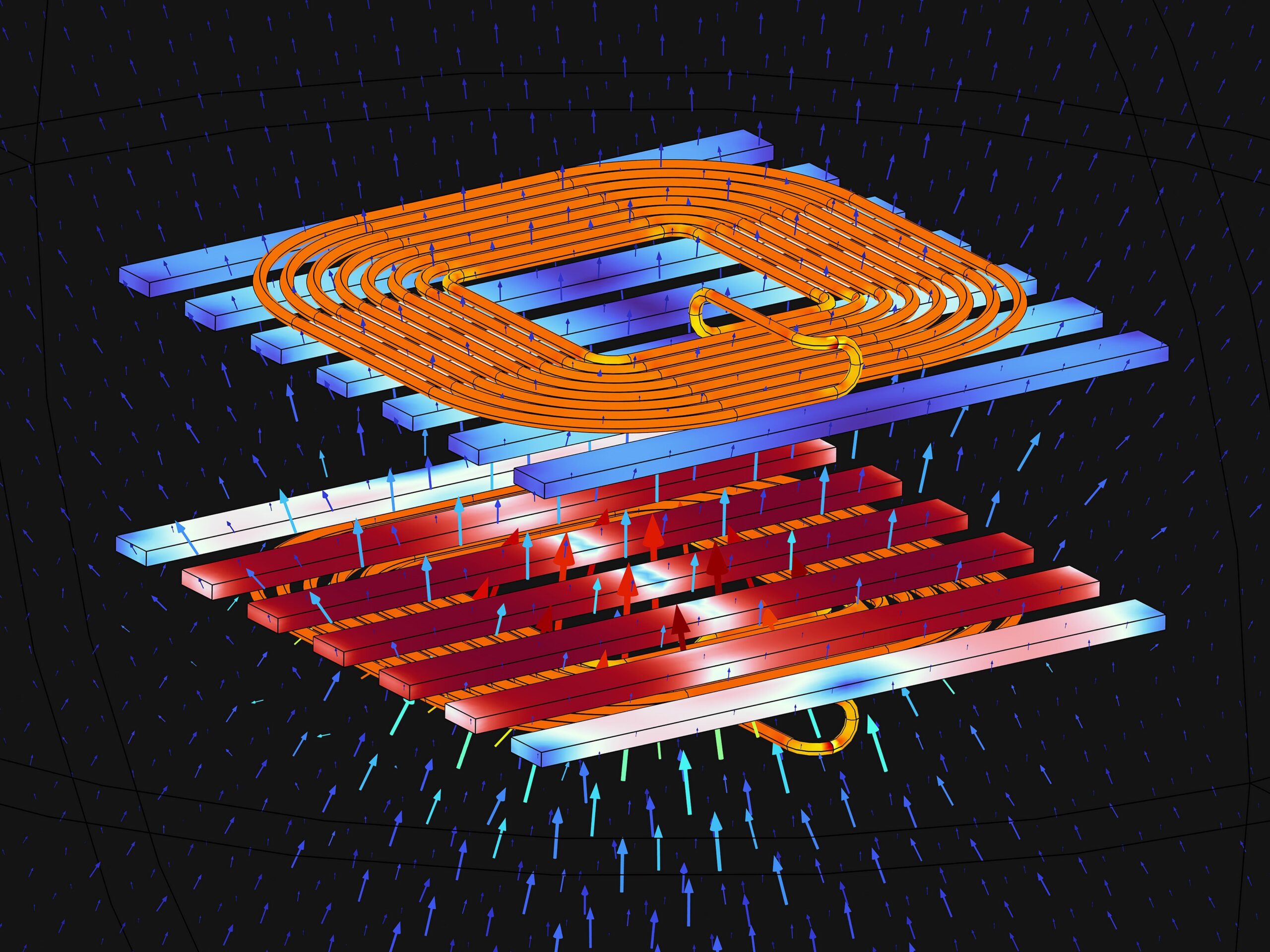
    Wireless connectivity is standard across corporate campuses, in warehouses and factories, and even in remote locations. But what about wireless power? Can we get rid of all cables?

    Many of us are already using wireless chargers for our cellphones and other devices. But induction chargers aren’t a complete solution since they require very close proximity between the device and the charging station. So, what can enterprises try? Some organizations are deploying midrange solutions that use radio signals to transmit power through the air, and others are even experimenting with laser power transmission.

    Here are three emerging options for wireless power in the enterprise, and top use cases to consider.

    Induction charging

    Induction charging is about more than saving users the two seconds it would take them to plug a cord into their device. It can also be used to power vehicles, such as factory vehicles, or even cars and buses. Also known as near-field charging, it’s the single largest sector of the global wireless power market, according to Coherent Market Insights, accounting for 89% of 2025’s $16.6 billion wireless power market. Of that, consumer electronics accounted for 74%.

    Detroit launched its first electric roadway in 2023, allowing vehicles to charge their batteries wirelessly when they park on, or drive over, that particular section of the road. It requires special equipment to be installed in the vehicle, and it can be pricy for individual cars, but it can be a useful option for buses or delivery vans. The city plans to add a second segment next year, reports the American Society of Civil Engineers.

    The first commercial user will be UPS, which will also add stationary wireless charging at its Detroit facility. “This innovative approach will revolutionize how we power our electric vehicles and drive fleet electrification forward,” said Dakota Semler, CEO and co-founder of electric vehicle manufacturer Xos, in a press release.

    Florida plans to open an electrified road in 2027, and, in California, UCLA is testing an in-road inductive charging system for campus buses that is planned to be in operation by 2028. The goal is to have the project ready in time for the 2028 Olympics Games in Los Angeles.

    Utah plans to add in-motion charging lanes to streets in the next ten years, and the first one scheduled to be installed later this year, as part of its electrified transportation action plan. A major impetus is the 2034 Winter Olympics, which will be held in Salt Lake City.

    Early adopters in Utah include Utah PaperBox and Boise Cascade’s Salt Lake distribution hub. There’s also an electrified roadway, currently in the pilot and development phase, at the Utah Inland Port, which will provide in-motion charging for freight vehicles. Construction of the world’s first one-megawatt wireless charging station has already begun at this facility, which will provide 30-minute fast charging to parked electric semi trucks.

    Europe is even further ahead. Sweden began working on the first electric road in 2018. In 2021, the one-mile stretch of electrified road was able to charge two commercial vehicles simultaneously, even though they had different battery systems and power requirements. In 2022, an electric bus began operating regularly on the road, charging while driving over it.

    The idea is that wireless in-motion charging will allow commercial vehicles to spend more time on the road and less time parked at charging stations — and less wasted time driving to and from the charging stations. It also allows vehicles to have smaller batteries and wider ranges. If the technology goes mainstream on public roads, drivers would be able to pay for the electricity they get in a way similar to how the E-Z Pass system works. But a more immediate application of the technology is the way that UPS is deploying — to charge up vehicles in a corporate facility.

    There are several vendors that offer this technology:

    • HEVO offers wireless charging pads for garages and parking lots for both residential and commercial markets.
    • Plugless Power is another company offering wireless charging for parked vehicles, and claims to have provided 1 million charge hours to its customers, which include Google and Hertz. It provided the first wireless charging stations for Tesla Model S cars, and its wireless charging system for driverless shuttlebuses was the first of its kind in Europe.
    • WAVE offers wireless charging system for electric buses, and its Salt Lake City depot can charge multiple vehicles automatically using inductive power. In addition to buses, other uses cases include ports such as the Port of Los Angeles, and warehouse and distribution. In warehouses, it can provide power to electric yard trucks, forklifts, and other equipment.
    • InductEV offers high-power, high-speed wireless charging for commercial vehicles such as city buses, auto fleets and industrial vehicles, with on-route wireless charging solutions deployed in North America and Europe. It was named one of Time magaaine’s best inventions of 2024. Seattle’s Sound Transit plans to have nearly half of its electric buses being charged by on-route wireless chargers from InductEV, and municial bus charging is already operational in Indianapolis, Martha’s Vineyard, and Oregon. The AP Moeller Maersk Terminal in Port Elizabeth, NJ is also using the company’s wireless chargers for its electric port tractors.

    Other companies offering wireless charging for industrial vehicles such as automated guided vehicles and material handling robots are Daihen, WiTricity, and ENRX.

    Meanwhile, cellphone charging pad-style wireless chargers also have plenty of business applications other than ease of use. Mojo Mobility, for example, offers charging systems designed to work in sterile medical environments.

    Ambient IoT and medium-range charging

    The most common type of ambient IoT is that powered by solar cells, where no power transmission is required at all. For example, ambient IoT is already reshaping agriculture, with solar-powered sensors placed in fields, greenhouses, and livestock areas, according to a September report from Omdia. Small devices can also be powered by motion or body heat.

    Transmitted wireless power, however, is more predictable and reliable and can work in a wider variety of environments — as long as the device is within range of the power transmitter or has a battery backup for when it’s not. Medium-range charging can work at a distance of a few inches to several yards or more. The less power the device requires, and the bigger its antenna, the longer the distance it can support.

    “It’s really pushing IoT to the next level,” says Omdia analyst Shobhit Srivastava.

    One popular use case is for sensors that are placed in locations where it’s not convenient to change batteries, he says, such as logistics. For example, Wiliot’s IoT Pixel is a postage stamp-sized sticker powered by radio waves that works at a range of up to 30 feet. Sold in reels, the price is as low as 10 cents a sensor when bought in bulk. The sensors can monitor temperature, location, and humidity and communicate this information to a company network via Bluetooth.

    Sensors such as these can be attached to pallets to track its location, says Srivastava. “People in Europe are very conscious about where their food is coming from and, to comply with regulations, companies need to have sensors on the pallets,” he says. “Or they might need to know that meat has been transported at proper temperatures.” The smart tags can just be slapped on pallets, he says. “This is a very cheap way to do this, even with millions of pallets moving around,” he says.

    The challenge, Srivastava says, is that when the devices are moving from trucks to logistics hubs, to warehouses, and to retail stores, “they need to connect to different technologies.”

    Plus, all this data needs to be collected and analyzed. Some sensor manufacturers also offer cloud-based platforms to do this — and charge extra for the additional services.

    One wireless power company, Energous, is doing just that, with an end-to-end ambient IoT platform consisting of wirelessly powered sensors, RF-based energy transmitters, and cloud-based monitoring software. Their newest product, the e-Sense Tag, was announced in June. The company has sold over 15,000 transmitters, says Giampaolo Marino, senior vice president of strategy and business development, and includes two Fortune 10 companies — one in retail IoT and one in logistics and transportation — among its customers.

    The new tags will cost around $5 each, though the price is subject to change as the product is commercialized, Marino says. It’s a bit pricier than the disposable tags that cost under $1 each. But they will last for years, he adds, and can be reprogrammed.

    “Three years ago, it was science fiction,” Marino says. “Today, it’s something we’re deploying.” It’s similar to how we went from cable internet to Wi-Fi everywhere, he says.

    One use case that we’re not seeing yet for this kind of medium-range power transmission is factory robots. “We are far away from that,” says Omdia’s Srivastava. “The use cases are for low-power devices only.”

    Similarly, smartphones are also energy-hungry devices with their big displays and other components that draw power, he says. “So, smartphones won’t be ambient powered in any hear future,” he says. “But small wearables, like wristbands in a hospital, can be ambient powered.”

    Like a warehouse, a hospital is a controlled physical location where power stations can be installed to provide power to the IoT devices, enabling a wide variety of applications, such as monitoring heart rates, respiration, and other key health metrics.

    Who’s in charge of wireless power networks?

    Is wireless power transmission a networking task that falls within the purview of the IT department, or is it handled on the operational or business unit level? According to Srivastava, that depends on the scale of the deployment. “It’s a smaller deployment, with one or two locations to track, it might just say with, say, the logistics team,” he says.

    But for larger deployments, with thousands of devices, ambient IoT is about more than just the power — there’s also the data transmission. “Then the network and security teams should be involved,” he says.

    Other issues that might come up beyond data security include electromagnetic interference and regulatory compliance for RF exposure.

    According to Omdia’s Srivstava and Energous, some of the notable vendors in the space are: Everactive (wireless ambient IoT devices); Wiliot (battery-free IoT pixel tags); HaiLa Technologies (low power wireless semiconductor); ONiO (self-powered, batteryless solutions); Atma.io from Avery Dennison atma.io (connected product cloud); EnOcean SmartStudio (sensor and data management); SODAQ (low power hardware platforms); Lightricity (integration of energy-harvesting solutions into IoT systems); SML Group (retail RFID solution integrators); Sequans (integration of cellular IoT connectivity into ambient IoT systems); Powercast (both inductive and radio power transmission); Ossia (RF power using the FCC-approved Cota wireless power standard); and Minew (Bluetooth bridge and gateway to support Wiliot IoT Pixels).

    Laser charging

    For longer distances, lasers are the way to go.

    Lasers can be used to power drones and other aerial craft or collect power from remote wind turbines. It can also be used to send power to cell towers in areas where power cables are impractical to deploy.

    In May, DARPA achieved a new wireless power transmission record, recording more than 800 watts of power at a distance of over five miles. This technology can even collect power from space-based solar collectors and beam it down to Earth. In fact, it’s a bit easier to beam power up and down since there’s less atmosphere to get in the way. Caltech’s Space Solar Power Project demonstrated this in 2023.

    In space, there are no day-night cycles, no seasons, and no cloud cover, meaning that solar panels can yield eight times more power than they can down on Earth. The idea is to collect power, transform it into electricity, convert it to microwaves, and transmit it down to where it’s needed, including locations that have no access to reliable power.

    In April, startup Aetherflux announced a $50 million funding round and plans to have its first low-Earth orbit test in 2026. China is currently working on a “Three Gorges dam in space” project, which will use super heavy rockets to create a giant solar power station in space, according to the South China Morning Post.

    The European Space Agency is expected to make a decision at the end of this year on proceeding with its own space-based solar power project, called SOLARIS.

    The same technology can also be used to transmit power from one satellite to another, and we’re already seeing a race to build a power grid in outer space.

    Star Catcher Industries plans to build a space-based network of solar power collectors that will concentrate solar energy and then transmit it to other satellites, meaning that companies will be able to send up more powerful satellites without expanding their physical footprint. On-the-ground testing was conducted earlier this year, and the first in-orbit test will take place in 2026.

    “Demand is growing exponentially for small satellites that can do more, from onboard processing to extended-duration operations,” said Chris Biddy, CEO at satellite manufacturer Astro Digital, which became Star Catcher’s first customer in September.

    🛸 Recommended Intelligence Resource

    As UAP researchers and tech enthusiasts, we’re always seeking tools and resources to enhance our investigations and stay ahead of emerging technologies. Check out this resource that fellow researchers have found valuable.

    → EHarmony